
[ad_1]
This week, startup Metalenz introduced that it has created a silicon chip that, paired with a picture sensor, can distinguish objects by the way in which they polarize gentle. The corporate says its “PolarEyes” will be capable of make facial authentication much less susceptible to spoofing, enhance 3D imaging for augmented and digital actuality, support in telehealth by distinguishing several types of pores and skin cells, and improve driving security by recognizing black ice and different hard-to-see highway hazards.The corporate, based in 2017 and exiting stealth a yr in the past, beforehand introduced that it was commercializing waveguides composed of silicon nanostructures as an alternative choice to conventional optics to be used in cell gadgets.Metalenz not too long ago started a partnership with ST Microelectronics to maneuver its know-how into mass manufacturing and expects to be transport imaging packages someday within the second quarter of this yr, in keeping with CEO Robert Devlin.IEEE Spectrum spoke with Devlin final week to seek out extra in regards to the firm’s know-how and what it will likely be in a position to do when it will get into client arms.IEEE Spectrum: Earlier than we speak about your new polarization optics, briefly assist us perceive how your fundamental know-how works.Robert Devlin: We use normal semiconductor lithography on 12-inch wafers to create nanostructures within the type of little pillars. These constructions are smaller than the wavelength of sunshine, so by altering the radius of the pillars, we will use them to regulate the size of the optical path of the sunshine passing via. For the primary technology of this know-how, we’re working with near-infrared wavelengths, which transmits via silicon, fairly than reflecting as seen gentle would do.What’s the benefit of utilizing nanostructures over conventional lenses?Devlin: Our know-how is flat, for one. If you find yourself utilizing a curved lens to place a picture on a flat sensor, it’s a must to make all kinds of corrections utilizing a number of lenses and finely controlling the spacing between the lenses to make it work; we don’t have to try this. We can also carry the features of a number of conventional lenses onto one chip . And we will manufacture these lenses in the identical semiconductor foundries because the picture sensors and electronics utilized in digital camera modules.The iPhone face ID system, for instance, has three lenses: one diffractive lens, for splitting infrared gentle being projected onto your face right into a grid of dots, and two refractive, for collimating the lasers to mission onto the face. A few of these modules have an optical path that’s folded by mirrors, as a result of in any other case they’d be too thick to suit into compact areas required for client gadgets. With the single-chip flat optics, we will shrink the general thickness, and don’t want folded optical paths or mirrors in even probably the most space-constrained purposes. 3D mapping is one other infrared imaging utility that makes use of a number of lenses as we speak. Augmented actuality techniques must create a 3D map of the world round them in real-time, with the intention to know the place to put the digital objects. At present, these use a time-of-flight system—once more, working within the infrared a part of the spectrum—which sends out pulses of sunshine and occasions how lengthy they take to get again to the picture sensor. This method requires a number of refractive lenses to focus the outgoing gentle and a diffractive lens to multiply the sunshine to a grid of factors. Additionally they require a number of lenses on the imaging aspect to gather the sunshine from the scene. A number of the lenses are wanted to right for the curvature of the lenses themselves, some are wanted to verify the picture is crisp throughout the whole discipline of view. Utilizing nanostructures, we will put all of those features onto one chip.In order that’s what the chips you introduced do?Devlin: Sure, and the primary product to make use of our know-how, transport within the second quarter of this yr, might be a module to be used in 3D imaging.Initially for cell phones?Devlin: For client gadgets usually but additionally for cell phones.What about AR?Devlin: In fact, everyone seems to be eagerly ready for AR glasses, and the shape issue stays an issue. I feel what we’re doing—simplifying the optics—will assist clear up the shape issue downside. Individuals get suspicious in the event that they see an enormous digital camera sitting on somebody’s face. Ours might be very small, and, for this utility, infrared imaging is acceptable, it permits the system to grasp the world round it with the intention to meld the digital world with it. And it isn’t affected by adjustments in lighting circumstances.OK, let’s speak about what you’re saying now, the polarization know-how, your “PolarEyes.”Devlin: After we spoke a yr in the past, I talked about Metalenz desirous to not simply simplify present cell digital camera modules, however to take imaging techniques which were locked away in scientific laboratories, as a result of they’re too costly, complicated, or huge, and mix their optics right into a single layer that might be sufficiently small and low-cost sufficient for client gadgets.A kind of imaging techniques entails the polarization of sunshine. Polarization is utilized in industrial and medical labs; it may be used to see the place cancerous cells begin and finish, it could possibly in lots of circumstances inform what materials one thing is manufactured from. In trade, it may be used to detect options of black objects, the form of clear objects, and even scratches on clear objects. At present, full polarization cameras measure round 100 mm x 80 mm x 80 mm, with optics that may value a whole bunch of {dollars}.
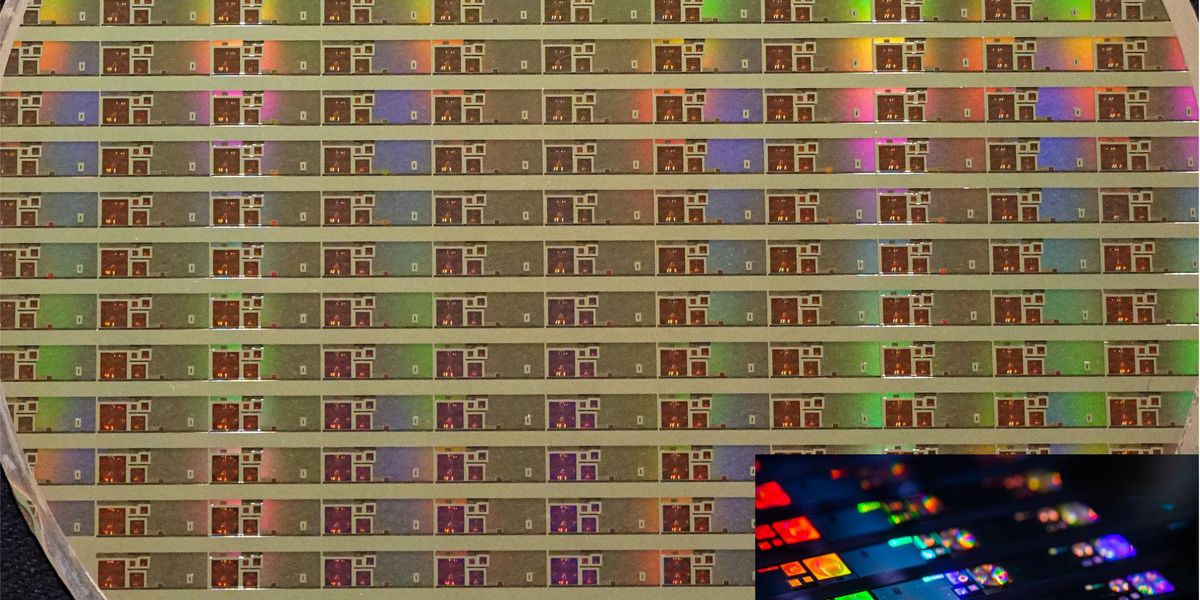
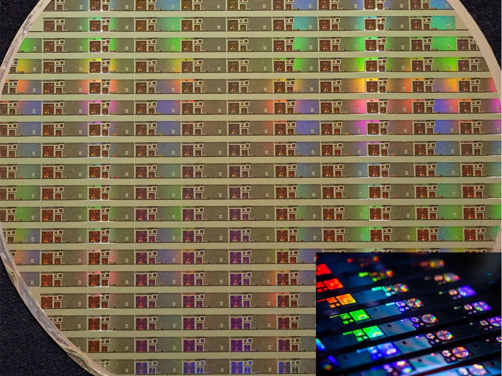
The PolarEyes chip from Metalenz kinds gentle by its polarization, permitting the pixels of photos captured to be color-coded by polarization. On this case, the distinction in polarization between supplies makes it apparent when a masks obstructs pores and skin.MetalenzUsing metasurface know-how, we will carry the dimensions down to three mm x 6 mm x 10mm and the worth all the way down to $2 to $3. And in contrast to many typical techniques as we speak, which take a number of views at completely different polarizations sequentially and use them to construct up a picture, we will use certainly one of our chips to take these a number of views concurrently, in actual time. We take 4 views—that seems to be the quantity we have to mix into a traditional picture or to create a full map of the scene color-coded to point the whole polarization at every pixel.In addition to the medical and industrial makes use of you talked about, why else are polarized photos helpful? Devlin: Once you get these into cell gadgets, we’ll seemingly discover all kinds of purposes we haven’t considered but, and that’s actually thrilling. However we do have an preliminary utility that we expect will assist get the know-how adopted—that’s in facial recognition. At present’s facial recognition techniques are foiled by masks. That’s not as a result of they couldn’t get sufficient info from above the masks to acknowledge the person. They use a high-res 2D picture that gives sufficient knowledge to the algorithms to try this. However additionally they use a 3D imaging system that could be very low decision, it’s meant to just be sure you’re not making an attempt to spoof the system with a masks or {photograph}, and that’s what makes facial recognition fail when you’re carrying a masks. A polarization imaging module may simply distinguish between pores and skin and masks and clear up that downside.
[ad_2]